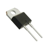

The STTH12T06DI is a 600V, 12A general-purpose diode in a TO220AC package, featuring a low forward voltage drop and very fast switching characteristics. Its primary applications include freewheeling, clamping, and snubbing in power conversion circuits such as switch-mode power supplies (SMPS), motor drives, and inverters. To maximize its performance and reliability, careful integration into the circuit and board layout is essential.
Recommended circuit topologies and design best practices center on leveraging its fast recovery for high-frequency operation. This diode is exceptionally well-suited for use as a freewheeling or flyback diode in flyback, boost, or buck-boost converters, and as a clamping diode in snubber networks across transformers or switching MOSFETs/IGBTs. In bridge rectifier configurations for offline power supplies, its fast recovery minimizes reverse recovery losses. A critical best practice is to always operate within the absolute maximum ratings, paying close attention to the junction temperature. The reverse recovery charge (Qrr) is a key parameter; minimizing the di/dt during turn-off through careful gate drive design for the associated switch can reduce stress and EMI. Always ensure the diode is placed as physically close as possible to the switching node it is protecting to minimize parasitic inductance in the loop.
Component selection guidelines for supporting passives are dictated by the diode's switching behavior. For RC snubber networks used to damp voltage overshoot, select a low-inductance, film or ceramic capacitor rated for high-frequency ripple current and a non-inductive, pulse-rated resistor. The values must be tuned empirically to critically damp the ringing without excessive power loss. For thermal management, a suitable heatsink must be selected based on the calculated power dissipation (Pdiss = VF * IF(AVG) + switching losses) and the thermal resistance from junction-to-ambient (RθJA). Use thermal interface material to mount the TO220AC package to the heatsink, and torque the mounting screw to the manufacturer's specification to ensure good thermal contact. A properly sized heatsink is non-negotiable for reliable 12A operation.
PCB layout recommendations and routing tips are paramount for high-speed switching components. The high-current loop formed by the diode, the switching transistor, and the bulk capacitor must be kept as extremely small and tight as possible. Use wide, short traces or preferably copper pours to minimize parasitic inductance, which causes voltage spikes and ringing. The diode's anode and cathode connections should use generous copper areas to aid in heat dissipation from the leads. If the diode is mounted on a remote heatsink, use multiple vias or a thick trace to connect its tab (which is electrically isolated in the INS version) to the appropriate copper plane for thermal relief. Keep sensitive analog or control traces far away from this high-dv/dt node to avoid noise coupling.
EMC/EMI considerations and mitigation strategies directly stem from the diode's fast switching. The rapid change in current during reverse recovery (high di/dt) can excite parasitic tank circuits, leading to conducted and radiated emissions. The primary strategy is to minimize the loop area as described above. Second, a well-designed snubber can dramatically reduce high-frequency ringing. Third, consider using a small ferrite bead in series with the diode's anode, placed close to the device, to damp high-frequency noise without affecting the main current pulse. Ensure input and output filters are properly implemented with decoupling capacitors close to the source of noise. Shielding may be necessary in severe cases, but a clean layout is the first and most effective defense.
Common design pitfalls and how to avoid them include: 1) Ignoring reverse recovery losses at high frequency, leading to unexpected thermal runaway—always calculate total losses including switching. 2) Inadequate heatsinking, assuming the package can handle the average current without derating—always design for worst-case operating temperature. 3) Poor snubber design, using inappropriate components or placing them too far from the diode, rendering them ineffective. 4) Assuming the tab is electrically connected—the "INS" suffix means it is isolated, so no insulating washer is needed, but thermal paste is still required. 5) Long, inductive traces causing destructive voltage spikes—revisit layout fundamentals to keep loops tight.
Prototyping tips and bench testing procedures should begin with a visual inspection of the board for proper solder joints and component orientation. Initially, power up the circuit with a current-limited supply and use a low input voltage. Probe the switching node with an oscilloscope using a short ground spring on the probe tip to observe the voltage waveform. Look for excessive overshoot or ringing, which indicates a need for layout improvement or snubber tuning. Monitor the diode's forward voltage drop with a known load to estimate conduction losses. Under full load, use a thermocouple or IR camera to measure the diode case temperature and ensure it is within safe limits, extrapolating to junction temperature using the thermal resistance. Finally, perform sweep frequency EMC pre-compliance tests to verify noise is within acceptable bands before final system integration.